In a development landscape as susceptible to rapid changes in technology and geopolitical factors as semiconductor design, IP security is becoming one of the industry’s foremost challenges. Though it is possible to maintain a secure work environment with traditional techniques, they tend to be highly restrictive, labor-intensive, and difficult to enforce and audit.
That’s why the best solution is a robust IP lifecycle management system that offers enterprise-grade security and complete traceability of your IP and its metadata across projects.
Common Risks to IP Security
IP security is paramount to the long-term success of your business, but the ever-evolving landscape of semiconductor design poses continual security challenges. Failing to implement comprehensive, proactive IP security measures can lead to significant long-term consequences. Some of the most prevalent IP security challenges today include:
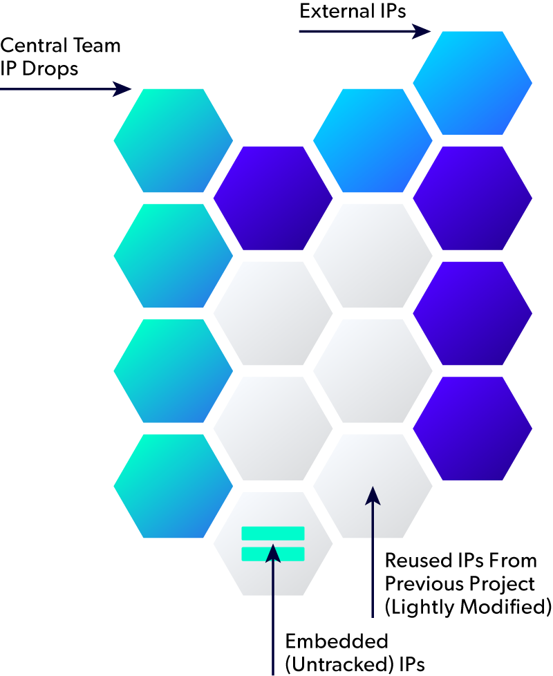
100s of Different IPs
The average SoC has more than 100 different IPs coming from many different sources. Some are developed internally, while others are from external vendors. This diversity poses significant IP security concerns, since each source presents potential vulnerabilities — from security breaches, to compromised functionality, to IP theft. How can you be certain that these IPs are safe?
IP Leakage
IP leakage — the unauthorized release of IP information to restricted locations and users — poses a significant risk. Leakage typically occurs as the result of mismanaging IP, whether through inadequate access controls, flawed use models, or a lack of traceability. With global trade complexities increasing, and violation of export control laws resulting in legal issues and millions of dollars in fines, preventing unintentional leaks is critical.
Global Uncertainties
Global uncertainties such as political conflicts, pandemics, climate change, and rising nationalism can disrupt supply chains and increase vulnerability to cyber attacks. Moreover, unstable geopolitical conditions hinder cooperation and regulation, making it difficult for companies to protect their intellectual property on a global scale.
Evolving IPs
IPs evolve as SoCs are developed. There are various feature changes and revisions that need to be incorporated into the design. With so many changes — and tight timelines — not every change can be thoroughly verified. As a result, some ‘minor’ changes are ignored or left to be tested later — and are often forgotten.
100s of Different IPs
The average SoC has more than 100 different IPs coming from many different sources. Some are developed internally, while others are from external vendors. This diversity poses significant IP security concerns, since each source presents potential vulnerabilities — from security breaches, to compromised functionality, to IP theft. How can you be certain that these IPs are safe?
IP Leakage
IP leakage — the unauthorized release of IP information to restricted locations and users — poses a significant risk. Leakage typically occurs as the result of mismanaging IP, whether through inadequate access controls, flawed use models, or a lack of traceability. With global trade complexities increasing, and violation of export control laws resulting in legal issues and millions of dollars in fines, preventing unintentional leaks is critical.
Global Uncertainties
Global uncertainties such as political conflicts, pandemics, climate change, and rising nationalism can disrupt supply chains and increase vulnerability to cyber attacks. Moreover, unstable geopolitical conditions hinder cooperation and regulation, making it difficult for companies to protect their intellectual property on a global scale.
Most design teams are multi-geographic and must grapple with these risks on top of all the other challenges of modern semiconductor design across globally distributed teams. But manually tracking and securing design assets is cumbersome, error-prone, and adds pressure to already stretched teams and schedules. A comprehensive, flexible, and scalable IP security solution has become a necessity in semiconductor design today.


What You Need in an IP Security Solution
To successfully assure IP security, you need the right solution that provides transparency and visibility across projects, fine-grained permissions, and complete traceability of your IP and its metadata from requirements to verification.
End-to-end traceability is critical to IP security. You need an IP security solution that can track all IP version usage, including both external and internally developed IPs, across projects and teams. Even when IPs are reused.
Here are some of the key functionalities you need to assure transparency and traceability for comprehensive IP security:
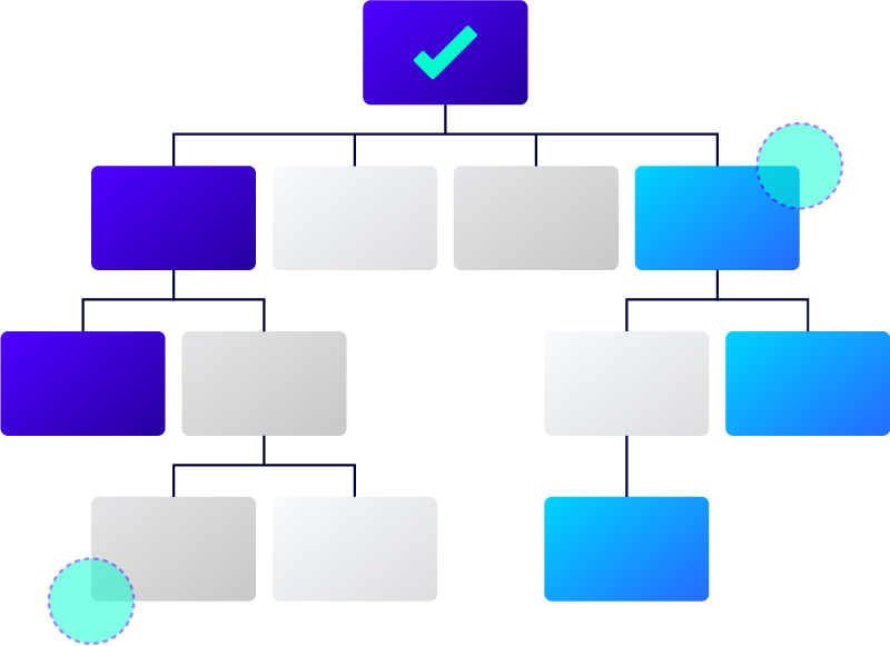
Bill of Materials (BoM)
A unified, hierarchical bill of materials is crucial in semiconductor IP security solutions as it provides a comprehensive view of every IP and component used in an IC or SoC, system, or platform, which may include software, hardware, and firmware. It enables precise tracking of the exact version of each IP in every platform variant and provides a complete, immutable view of the project, including all versions and dependencies. So, if a security vulnerability is found in an IP version or component, you can quickly assess everywhere it has been used.
IP Management
IP management is essential for securely storing, organizing, and sharing semiconductor IP, whether external or internally developed IPs. A robust IP management system facilitates efficient cross-functional and global collaboration while enforcing strict access controls through fine-grained permissions based on role and geography. This ensures designers can only access the IP that is available to them, preventing unauthorized use and IP leakage.
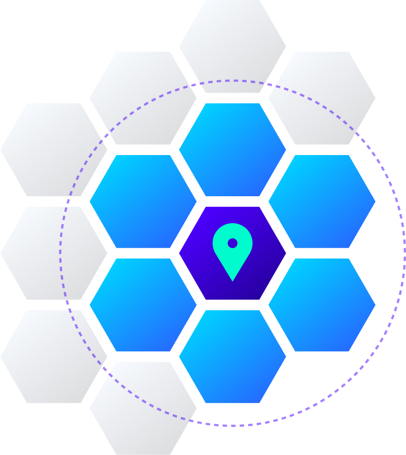
IP Geofencing
By defining virtual boundaries around authorized locations, IP Geofencing allows you to restrict IP availability and disable IP from residing in user workspaces in certain geographies, regardless of access permissions. IP geofencing is essential to prevent IP leakage to unauthorized regions, protect against export violation fines, and keep your organization in compliance with export control laws including EAR and ITAR – even amid rapidly shifting regulations.
Workspace Management
Description automatically generatedWorkspace management is important in an IP security solution, as it enables the creation and administration of secure work environments for design teams. Centralized, dynamic workspace management allows administrators to easily control which design files, IPs, tool configurations, and other infrastructure components are available to team members, to minimize the risk of IP exposure and ensure compliance with rapidly shifting security requirements.
Design Data Management
Secure, scalable design data management safeguards valuable IP by centralizing storage, versioning, and access control mechanisms for IPs and design files. This ensures that sensitive design data remains protected against unauthorized access, modification, or distribution throughout the product development lifecycle.
Analytics
Analytics functionality plays a crucial role in semiconductor IP security solutions by providing insights into user activities, access patterns, and potential security threats. By analyzing metadata, access logs, and usage metrics, organizations can identify anomalies, detect unauthorized access attempts, and proactively address security vulnerabilities to protect valuable IP assets from theft or leakage.
Integrations
Integration with other tools in the design workflow is also important for IP security. For example, an integration with a bug tracking tool like Jira will help you quickly understand which IP versions are affected when a security vulnerability is detected. Native integration with your underlying data management system is also critical to ensure consistent enforcement of access controls, metadata policies, and IP management procedures throughout the design process.
How Perforce Semiconductor Solutions Secure Your IPs
Perforce offers the only unified, scalable IP and data management solution that delivers all of the above security features that semiconductor design teams need, from a unified, versioned Bill of Materials to integrations with leading tools. Together, Perforce Helix IPLM and Helix Core make it easy to securely manage and track changes to all of your IP and its metadata over time with complete traceability.
Protect Your Critical IP from Every Angle
Collaborate Worldwide Without Compromise
Securely Manage All Design Data
9/10 Top Semiconductor Companies Trust Perforce
The world’s leading semiconductor companies rely on Perforce for enterprise IP security.


Talk to An IP Security Expert
Find out how secure, scalable IP and data management solutions from Perforce can help protect your IP across the globe. Get in touch with an IP security expert today.